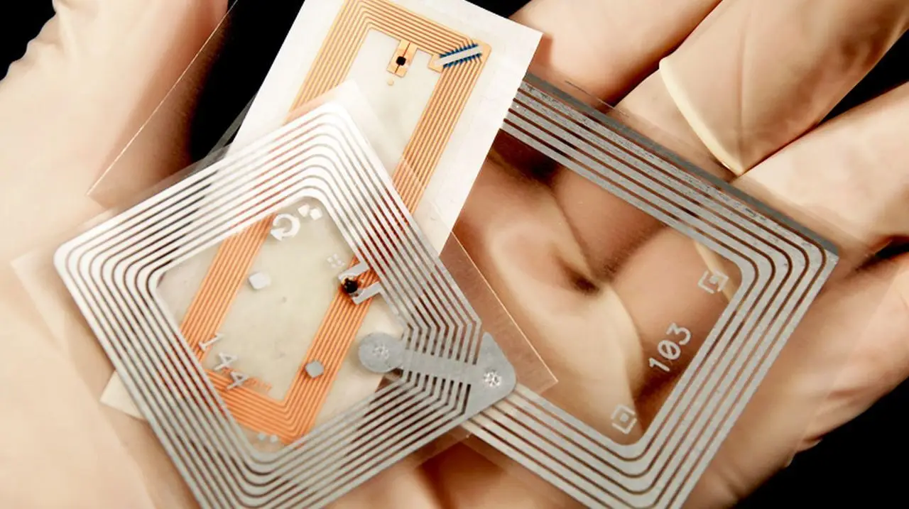
RFID Inlays
RFID inlays are versatile core components that enable efficient and reliable wireless communication tailored to diverse industrial applications through specialized frequencies, form factors, and manufacturing processes.
- Published: May 02, 2024
- By: Anja Van Bocxlaer
- Read: 4 min
- RFID inlays consist of a microchip and antenna enabling wireless communication in RFID and NFC systems.
- Various inlay types—UHF, HF, LF, and NFC—are optimized for different frequency ranges and application needs.
- Special form factors such as flexible, hard plastic, and miniaturized inlays address use cases in wearables, industrial environments, and compact devices.
- The production of tags from inlays involves design selection, integration into carrier materials, programming, and quality testing.
- A competitive market of manufacturers provides diverse inlay solutions tailored to enhance wireless system applications across industries.

What is an inlay?
An inlay is a thin layer consisting of a microchip and an antenna that serves as the core of RFID (Radio Frequency Identification) and NFC (Near Field Communication) tags. These components are designed so that they can be integrated into or applied to other materials to enable wireless communication.
Inlays are used in many industries, including logistics, retail, access control and many others.
What forms of inlays are there?
The variety of inlay shapes reflects the wide range of applications and requirements that need to be covered by these technologies. By customizing the shape and technology of inlays, companies can ensure that they get the most effective and efficient solutions for their specific needs.
Whether for logistics, access control, mobile payments or interactive marketing campaigns - the right choice of inlay is crucial for the success of the respective application.
UHF RFID Inlay
These inlays operate in the ultra-high frequency range (860-960 MHz) and offer a long range and high data transmission rates. They are commonly used in logistics and retail for inventory tracking and management. UHF RFID inlays can cover long distances and read multiple tags simultaneously, making them ideal for applications such as warehouse management and inventory control.HF RFID Inlay
High-frequency inlays (13.56 MHz) have a shorter range than UHF inlays, but offer better interference resistance and are ideal for applications that require a short communication distance, such as access control and ticketing systems.LF RFID Inlay
Low-frequency inlays (125-134 kHz) offer the shortest range, but are very robust against metallic environments and water. They are often used in applications such as animal identification and vehicle identification.NFC Inlay
NFC inlays are specially designed for near-field communication and also operate in the HF band (13.56 MHz). These inlays enable wireless communication between devices over very short distances (up to 10 cm). They are available in various forms, includingCard shaped inlays: These inlays are often integrated into credit cards or access cards and enable contactless payments and access control.
Sticker inlays: These flexible inlays can be applied to various surfaces, including posters, products or packaging, to enable interactive marketing campaigns or product tracking.
Key fob inlays: These robust inlays are ideal for applications where user-friendliness and durability are paramount, such as key cards for hotels or fitness studios.
Special Form Factors
Flexible Inlays
These inlays are applied to flexible substrates and can be integrated into textiles or clothing. They are ideal for wearables and smart clothing.Hard plastic inlays
These robust inlays are designed for harsh environments and can be used in industrial areas where resistance to physical influences is required.Miniaturized inlays
Small inlays are suitable for compact applications such as medical devices or small electronic products where space is limited.
Which technologies are used for inlays?
RFID
The RFID technology uses electromagnetic fields to identify and track objects. RFID inlays can communicate over greater distances than NFC inlays and are often used in inventory management and logistics.
NFC
NFC is based on RFID technology, but is optimized for close range. NFC inlays enable secure and fast data transfer between devices and are frequently used in mobile communication and contactless payment systems.
Bluetooth LE
BLE inlays can communicate over greater distances than NFC and some RFID types and consume very little energy.
How does an inlay become a tag?
Design and production
The first step is to design the inlay. This includes selecting the right chip and antenna as well as determining the optimum size and shape. Production usually takes place in specialized production facilities that have the necessary technology to precisely combine the sensitive components.
Integration
The finished inlay is integrated into the carrier material. This can be a plastic card, a paper label or even a textile, depending on the application requirements. The integration process can include laminating, gluing or embedding the inlay.
Programming and testing
The final tag is programmed and tested to ensure that it meets the desired specifications. This includes encoding the desired data on the chip and testing the antenna performance.
Finishing
Depending on the application, the tag can be further processed, e.g. by printing, cutting or adding protective layers.
Which inlay manufacturers are there?
The market for RFID and NFC inlays is highly competitive and there are several leading manufacturers offering high-quality products. Wireless inlays, especially RFID and NFC inlays, are essential components of modern wireless communication systems. They enable a wide range of applications, from inventory management to access control and mobile payments.
With a wide range of shapes, technologies and leading manufacturers, the inlay market offers numerous possibilities to meet the individual requirements of different industries. By choosing the right inlays and partners, you can significantly increase the efficiency and safety of your applications.

