- ASML’s EUV lithography systems are essential for printing nanometer-scale integrated circuits on silicon wafers.
- The technology required over 20 years of research and close collaboration with European partners to develop.
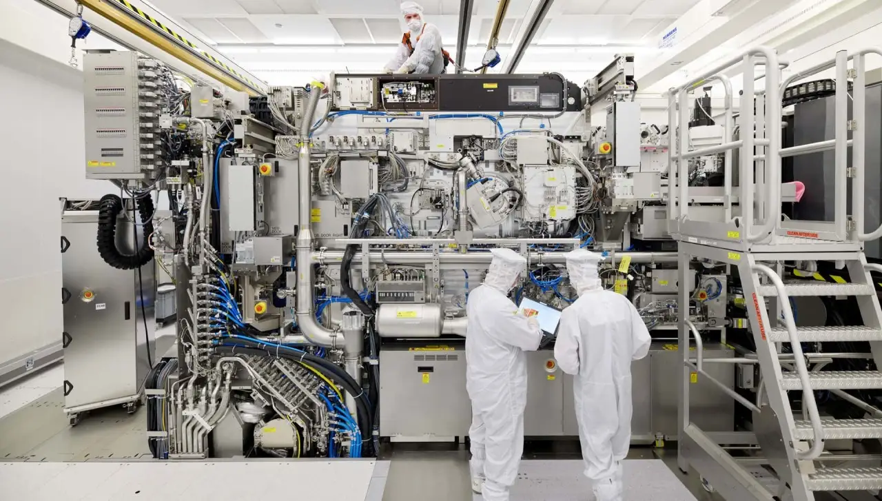
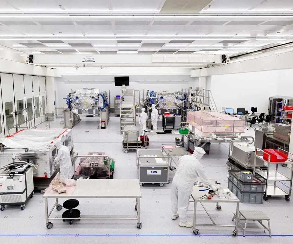
- Each EUV machine contains approximately 100,000 parts and takes months to manufacture in cleanroom environments.
- ASML regularly provides hardware and software upgrades to existing lithography systems to maintain competitiveness.
ASML was founded in 1984 between ASM International and Philips Electronics as a joint venture. Its headquarters in Veldhoven, the Netherlands, and a subsidiary in Arizona were established in 1985.
The year 1986 was outstanding from a strategic point of view, as ASML launched the first semiconductor imaging system and began its long-standing development partnership with German optics company Carl Zeiss. Since 1995, ASML has been listed on the AEX and NASDAQ. ASML’s EUV (Extreme Ultra Violet) lithography systems are the world’s most advanced equipment for the mass production of chips.
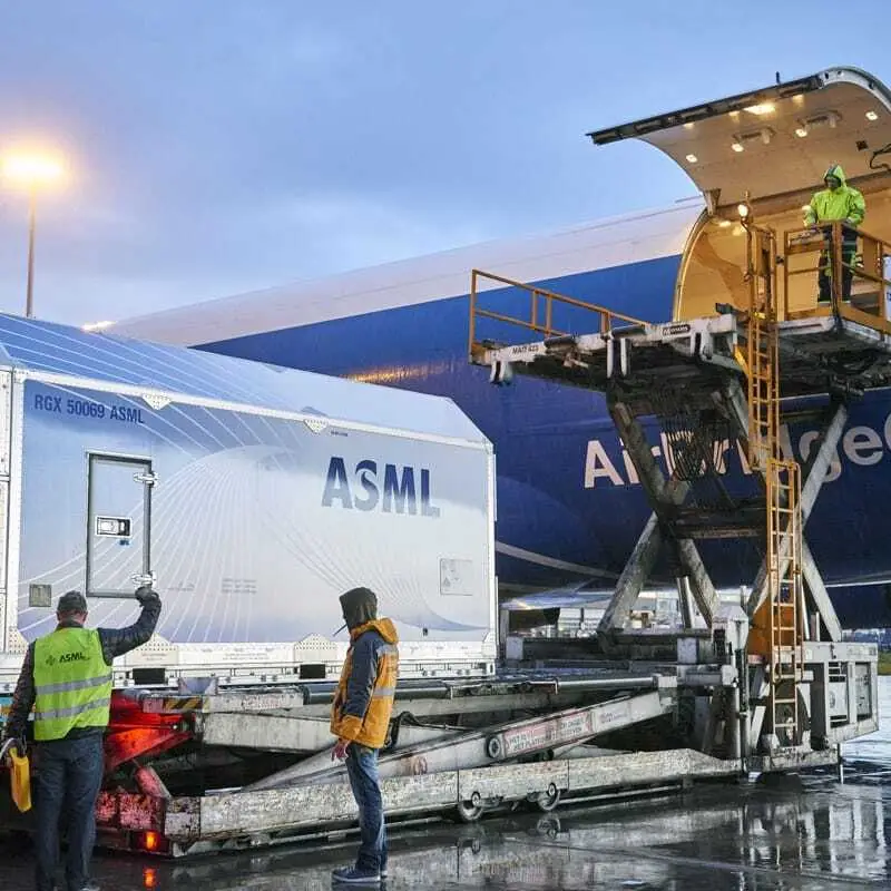
ASML successfully introduced this technology to its customers after more than 20 years of continuous research and development. Chipmakers have been using EUV for the most advanced chip manufacturing since 2016. Each machine consists of 100,000 parts and modules, is approximately the size of a bus and requires three transport aircrafts for delivery.
Interview with Sander Hofman
Interview
1. Can you briefly describe ASML as a company?
Sander Hofman: ASML is a leading supplier to the semiconductor industry. We provide chipmakers with lithography machines, software and services to mass produce the patterns of integrated circuits (microchips). We were founded as a joint venture in 1984 and spent the first ten years of our company's history to make a competitive lithography machine—and a name for ourselves. In its early years, ASML was dependent on subsidies and support programs from the Dutch government and the European Union.
By the early 1990s, we had a system that started to sell to the biggest chipmakers in the world. They were impressed by the resolution, small footprint and modularity of the system. That modularity was born out of how we do business: we don’t innovate in isolation. We are architects and integrators. We develop our technology in close collaboration with our customers and technology partners, while we trust our supply chain to manufacture most system parts and modules. Many of our strategic partners are based in Europe. These include Carl Zeiss in optics and Trumpf in laser technology, among others.
2. How is the “know-how” of ASML protected?
Hofman: We now hold over 15,000 patents for a wide variety of technologies. The patents cover not only the main business, lithography, but also other relevant markets. This applies to, for example, metrology, measuring instruments for evaluating lithography, and computer-aided lithography. This includes the aspects machine learning and AI.
Even though ASML was originally a hardware company, the software sector has become an essential part of our innovation over the past decade. The knowledge is proprietary and crucial for the functions of the machines at the nanometer level.
3. What functions do ASML’s machines perform in semiconductor manufacturing?
Hofman: Let's say we take a phone apart into its individual components. Inside are numerous chips that perform different functions. In the case of the iPhone, for example, this is the famous A15, or the M1 in the Mac. These chips are the brains of the device.
If you were to take a closer look at this chip, you would see hundreds of layers of interconnected geometric patterns. Together, these form an integrated circuit or chip. All these layers of patterns are what our machines can print on silicon. Production must take place in cleanroom environments.
4. How long does it take to manufacture the machines?
Hofman: Semiconductor manufacturers operate their factories 24 hours a day, 365 days a year. And the same is true for ASML. The cleanroom environments where the systems are manufactured operate 24 hours a day, so our people work in shifts. The manufacturing process is quite time-intensive. For older generation machines, the production can take weeks.
But for an EUV system, it will take months. The supply chain needs to deliver all parts and modules on time as well, which is a logistical challenge in and of itself. Assembling and testing the machines also takes time. With the current chip shortage still going on, we are ramping up our production capacity.

Printing Patterns on Silicon Wafers Using EUV Light
Integrated Circuits
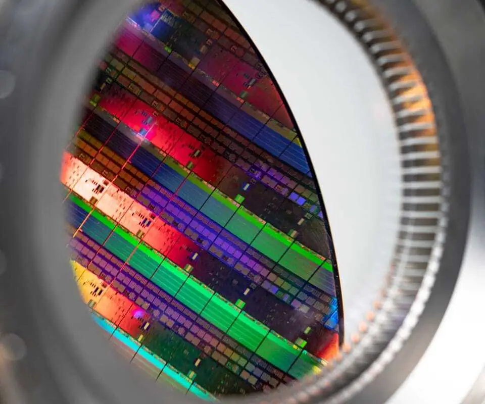
Integrated circuits can comprise of billions of components, so that even highly complex circuits can be accommodated on silicon of just a few square millimeters in size. Manufacturing involves a large number of individual physical and chemical processes. Since the performance of microprocessors generally increases as the structures on the chip become smaller, their degree of miniaturization is often at the limit of what is technically and physically possible.
Interview
5. What exactly is lithography?
Sander Hofman: An integrated circuit or chip consists of hundreds of layers of interconnected patterns. Our machines print these patterns on silicon. In simple terms, ASML's machines are advanced copiers for these patterns. This process is called lithography. In the machines, we have a light source, with light of a certain wavelength. In the case of EUV systems, the newest and most innovative systems, this is already in the name – EUV, Extreme Ultra Violet Light, with a wavelength of 13.5 nanometers.
6. What is the significance of light for production?
Hofman: The light with a wavelength of 13.5 nanometers is generated by us and directed through our machines via optics. These mirrors are manufactured by ZEISS in Germany. The light is reflected by a master pattern that we call a "mask." This encodes the pattern into the light beam. Finally, the light beam with the pattern now encoded in it are shrunk in size using further optics before it lands on a photosensitive silicon wafer, essentially printing it onto the surface repeatedly, like a copier.
7. What are the final production steps for the wafer?
Hofman: After lithography, the wafer is further processed in the semiconductor factory of our customers. These additional steps are done with machines from other suppliers of semiconductor equipment. The wafer is treated with chemical baths, etched and ionized, among other processes, for finalization. In total, it can take up to three months for a wafer to make its rounds through a customer's fab.
Multiple layers have to be printed, one on top of the other, the wafer etched again and processed with lithography. The result is a silicon wafer on which hundreds, sometimes thousands, of chips are printed side by side. The final product can then be cut into individual chips and packaged before being incorporated into electronic devices. This is the basic context for what our machines are and how they work.
Technological Features of EUV-Systems
Technological Features of EUV-Systems
Lithography requires extreme mechatronics engineering. The motion of the mask and wafer must be perfectly synchronized, but because the chip pattern on the mask is larger than the resulting pattern on the wafer, the reticle must move much farther and faster, up to 150 meters per second squared. That’s the equivalent of a car accelerating from 0 to 100 km/h in just 0.1 seconds.
The ability to synchronize the motion of wafer and reticle to the nanometer and nanosecond as they accelerate at 5 g and 15 g in opposite directions – all without causing a single vibration – is vital for producing functioning microchips.
Interview
8. What are the unique features of ASML’s EUV machines?
Sander Hofman: The EUV systems are unique in their complexity, in the way they are developed and how ASML works with the supply chain to manufacture them. Ultimately, what matters is that the chip industry demands an affordable machine, which can achieve the highest performance for the layers of chips in semiconductor manufacturing that have the smallest features. EUV technology enables the most advanced semiconductor manufacturing.
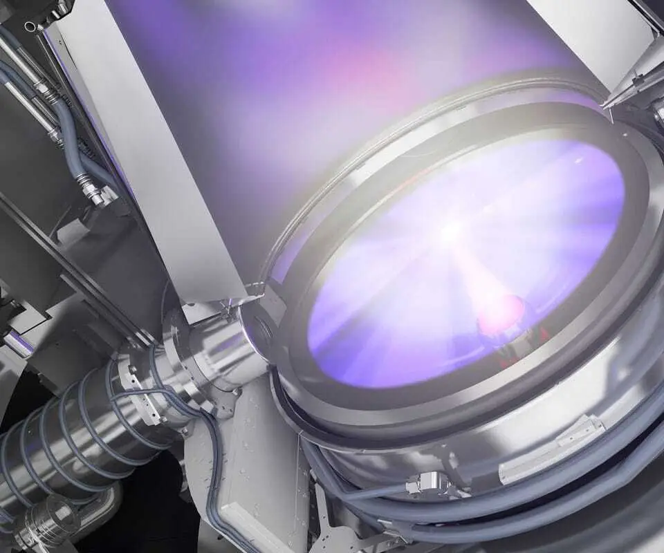
9. How is the light generated in the EUV machine?
Hofman: Light generation in EUV lithography is an incredibly complex process. A generator ejects 25-micrometer tin droplets at a speed of 70 meters per second inside a vacuum vessel. Trumpf manufactures a very powerful industrial CO2 laser for the system, which is fired at these tin droplets. Each individual droplet must be hit twice. The first hit occurs with a low intensity laser pulse that flattens the tin droplet, similar to the shape of a pancake. The second hit with a stronger laser pulse vaporizes the droplet and generates EUV light.
A vacuum is required in the EUV machine because extreme ultra violet light is absorbed by all materials. For this reason, mirrors are used instead of lenses, as mirrors can reflect and transmit the light. This is the only way to direct the light through the machine and onto the wafer, as lenses would simply absorb it.
10. What were the biggest challenges in the development of the EUV machines?
Hofman: The development of the light source, vacuum technology and optics in EUV were enormous challenges. This is why the development took 20 years. ASML and its suppliers had to master these phenomena at the fundamental level of physics before being able to engineer for them. During this process, new problems and tasks kept arising that had to be solved. However, in the end, ASML mastered the physics of the technology and was able to engineer for it. The result is a functional EUV machine that performs its tasks reliably and precisely in a customer fab.
System Upgrades and Development for the Future Semiconductor Market
Interview
11. What upgrades does ASML offer for existing systems?
Sander Hofman: ASML offers hardware and software upgrades. As defined in the roadmap, large initial deliveries of systems are executed and upgrades are offered approximately every couple of yearly quarters. This is an immense advantage of the modularity of the machines, which has proven to be a success factor for ASML over the years. ASML offers chip manufacturers a platform on which they can purchase the system with exactly the configurations needed for their specific chips. ASML regularly develops and offers upgrades. Upgrades can for example increase system productivity or offer more precision in mass production.
12. Do the upgrades involve downtime in production?
Hofman: The rollout of software is usually very easy and fast, while hardware upgrades can take days or weeks, depending on the type of upgrade. ASML's systems receive upgrades on a regular basis. It requires some downtime that is coordinated with the semiconductor manufacturers. This makes all the difference. As manufacturers run a highly automated fab, there are numerous different processes with multiple machines. Planned downtime ensures that disruption to production is kept to a minimum.
13. Do older generations of ASML's lithography systems also receive upgrades?
Hofman: Over 95 % of all systems ever manufactured by ASML are still in use today. The older systems are used in the production of chips with larger features and transistor sizes suitable for automotive or sensor applications. The market for semiconductors is booming in these application areas. We have systems in our product portfolio that are made specifically for these applications, with the service and upgrades that go with it. Some of our oldest systems are refurbished.
Interview
14. How many EUV machines does ASML manufacture each year?
Hofman: In 2021, ASML shipped a total of 286 lithography systems, which included around 40 EUV systems. Currently there is a semiconductor shortage, with a huge demand driven by major trends such as 5G, AI and Big Data, Internet of Things, and autonomous driving. Production across ASML’s entire portfolio is set to increase. For EUV in particular, this means that a capacity of 55 systems is targeted for 2022. For the following year, ASML aims to produce 60 EUV systems.
15. What developments to you foresee for the semiconductor industry and ASML?
Hofman: As far as the development of the semiconductor industry and transistor sizes of chips are concerned, the answers can be found in the roadmaps of companies like Intel, TSMC and Samsung. These companies plan to shrink transistor sizes for the next decade and beyond. In part, this development is possible because ASML continues to fuel innovation with its EUV system.
ASML is already working on the next generation EUV platform, which will offer an even finer resolution. Mass production is expected to start in 2025. The supply chain is working actively to provide all components and modules that will come together in the ASML cleanroom in Veldhoven to build the first machine. The shrinking of transistor sizes is progressing rapidly and there is the industry appetite for it. There is chip in everything now, more so than ever before. There has also been an increase in all kinds of automotive solutions and sensor technology. The chip industry is booming, and we stand to offer the tools to push innovation forward.
16. How is ASML preparing for the changes in the chip industry?
Hofman: Crucially, if you look at the semiconductor market, there is a massive boom right now. Total industry sales are currently around $550 billion, and forecasts suggest that this could grow to $1 trillion by the end of the decade. ASML is currently expanding its production capacity. More space is being used and more employees are being hired to produce more machines faster. New cleanrooms are being built. This is an ongoing trend that can also be seen among ASML's strategic partners and suppliers.
Together, we are working on the next generation of lithography systems, while we’re also innovating the current generations. In my opinion, these are exciting times. We are entering an era where the semiconductor industry is at the center of a tremendous amount of innovation that will move the world forward. And hopefully it will help solve some of the problems we are dealing with as humanity, like climate change, access to healthcare, and education equality. Technology can help address these challenges in ways that have never before been possible.