- Gallium nitride enhances RF power amplifiers with higher efficiency and power density, critical for 5G and future wireless networks.
- GaN is widely adopted in high-performance 5G macro base stations and active antenna arrays to support massive MIMO technology.
- Research is advancing GaN for 6G with components designed for mmWave and sub-terahertz frequencies, enabling more compact and efficient devices.
- Industrial production is shifting towards GaN-on-silicon to reduce costs and enable scalable manufacturing for wireless communication hardware.
- GaN also benefits satellite communication, wireless backhaul, radar systems, and supports more sustainable network operations through energy savings.
When talking about the future of wireless communication today, terms such as 6G, terabit networks, satellite internet, and sub-terahertz frequencies quickly come to mind. But behind these visions lies a very concrete technological foundation: powerful high-frequency electronics. This is precisely where a semiconductor material is increasingly becoming the center of attention – gallium nitride (GaN).
Just a few years ago, GaN was primarily considered a special technology for radar or defense systems. Today, the material has already found its way into many 5G base stations and is developing into one of the key technologies for future wireless networks.
Research institutions such as the Fraunhofer Institute for Applied Solid State Physics IAF and the Belgian nanoelectronics center imec are driving development forward, as are companies in the semiconductor industry.
From niche technology to 5G reality
The most important area of application for GaN is currently in RF power amplifiers – i.e., the amplifiers that generate radio signals from base stations or satellite antennas. Silicon or gallium arsenide components were long the norm in classic mobile networks. However, the transition to 5G has drastically changed the requirements.
Modern mobile stations operate with massive MIMO (multiple input multiple output) antennas , in which dozens or even over a hundred antenna elements transmit and receive simultaneously. Each of these elements requires its own amplifier. This significantly increases power consumption and heat generation.
This is where GaN is already demonstrating its advantages: the material enables higher power density and better efficiency, meaning that less energy is lost as heat. For network operators, this not only means lower operating costs, but also more compact hardware and less cooling.
Many manufacturers are therefore already relying on GaN-based power amplifiers in mobile communications infrastructure. Today, their use is particularly widespread in high-performance macro base stations and active antenna arrays.
Industry drives GaN into radio infrastructure
While research institutions are developing new GaN technologies, the semiconductor industry has already established the material on a large scale in radio infrastructure. Companies such as Infineon, Qorvo, and Wolfspeed are developing and producing GaN-based high-frequency components for mobile communications base stations, satellite communications, and radar.
The biggest advantage lies in the combination of high power density, efficiency, and frequency capability. Especially in massive MIMO antennas with many parallel transmission and reception paths, GaN amplifiers can help reduce power consumption and cooling requirements.
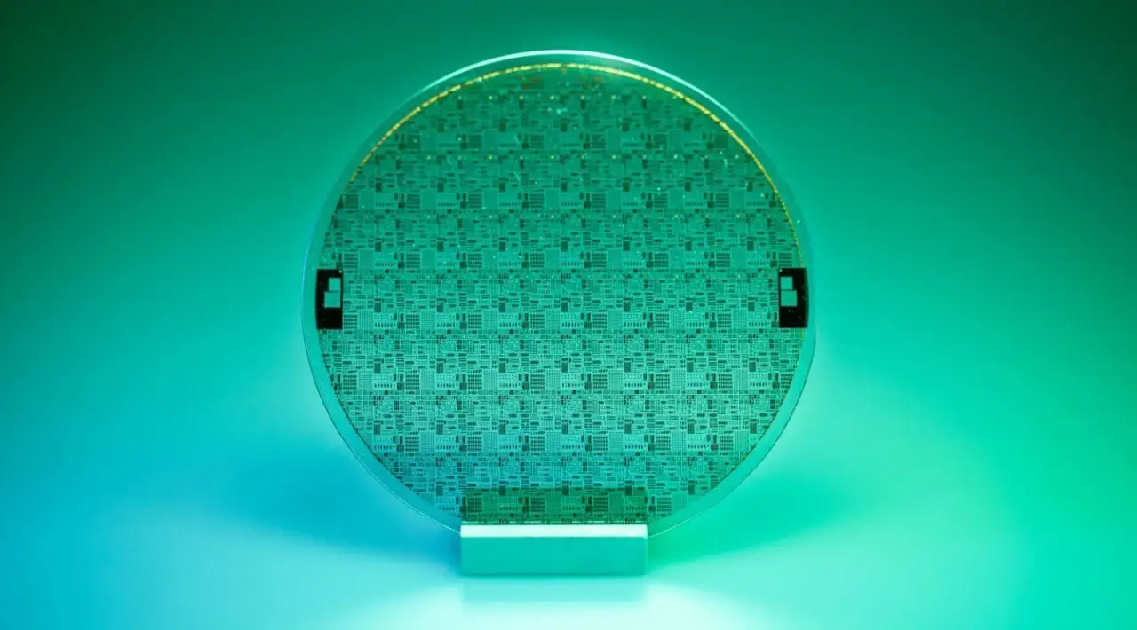
At the same time, the industry is working on scaling the technology economically. In addition to the established GaN-on-SiC technology, which enables particularly high performance, GaN-on-silicon processes are also increasingly emerging. These can be manufactured on larger silicon wafers, opening up the possibility of more cost-effective mass production for wireless hardware in the long term.
Research is driving GaN toward 6G
While GaN is already established in the 5G network, research is working on further developing the technology for the next generation of mobile communications.
At the Fraunhofer Institute for Applied Solid State Physics IAF, GaN-based high-frequency components are being developed that reach frequencies far beyond today's mobile communication bands. The goal is to develop applications for mmWave and future sub-THz communication systems, which are being discussed for 6G.
At the same time, imec is working on new GaN transistor structures that achieve high performance and efficiency at comparatively low operating voltages. Such components could also be used in more compact RF front ends or even mobile devices in the future.
This development clearly shows that while GaN was originally intended primarily for high-performance applications, the material is also becoming increasingly interesting for scalable and integrated wireless architectures.

Scaling: From special material to industrial platform
A crucial step for the future of GaN lies in industrial manufacturing. For a long time, many GaN components were manufactured on silicon carbide substrates (GaN-on-SiC). This technology offers excellent electrical and thermal properties, but is relatively expensive.
That is why the industry is increasingly working on GaN-on-silicon technologies that can be produced on conventional silicon wafers. This approach enables larger wafer sizes and better integration into existing semiconductor manufacturing.
If this approach prevails, GaN could become significantly cheaper and more widely available in the coming years.
More than mobile communications: GaN is also changing satellite and IoT networks
The impact of the technology is not limited to traditional mobile networks. GaN is also becoming increasingly important in other areas of wireless communication.
One example is satellite communication. Modern low-Earth orbit constellations require powerful but compact antennas and amplifiers. Here, GaN enables high output power with comparatively low energy consumption – a decisive advantage in space.
The material is also playing an increasingly important role in future wireless backhaul connections, radar systems, and high-frequency microwave links.
Raw materials and sustainability
The question of the long-term availability of GaN depends primarily on the supply of gallium. Gallium is not a rare earth element and is not "extremely rare" geologically, but it is mainly obtained as a by-product – primarily from process streams in aluminum production (bauxite) and, to some extent, zinc processing. The decisive factor is therefore not so much whether gallium is available, but how much of it can be economically recovered and refined.
At the same time, the material requirements put the debate into perspective: GaN is usually used in semiconductor manufacturing as a very thin layer on a substrate, so that comparatively little gallium is required per wafer. Overall, it is fundamentally realistic to scale up supply – provided that recovery and refining are expanded in line with demand.
Ecologically, GaN's main impact is through efficiency: more powerful RF amplifiers can reduce the energy consumption of communication networks. Because mobile communications infrastructure runs 24/7, even small efficiency gains add up to noticeable savings over the lifetime of a network.
The silent revolution in the background of networks
GaN usually remains invisible to end users. Smartphones, routers, and IoT devices look no different just because a different semiconductor is used in the base station.
But in the background, the material is changing the architecture of modern wireless networks. More powerful antenna arrays, more efficient satellite links, and more compact radio modules are becoming possible without a corresponding increase in energy consumption.
With each new generation of wireless communication, the demands on frequency, performance, and efficiency grow. This is precisely why GaN is increasingly becoming the technological foundation of the next wireless generation.
The real revolution is not taking place in the device in your hand, but in the infrastructure that drives our connected world.