- Reinhard Jurisch conceived and patented the mic3 coil‑on‑chip approach that integrated antenna coils directly on silicon, enabling radical miniaturization.
- Non‑volatile memory (EEPROM) and mixed‑signal semiconductor design were critical enablers for battery‑free, writable transponders.
- Collaboration with industry partners, notably George Perlegos at Atmel, provided foundry capability and process rules that moved prototypes to production.
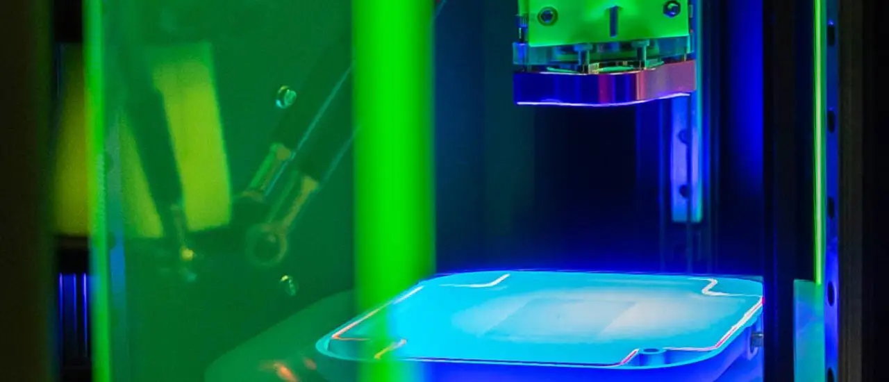
- Microsensys commercialized the mic3 technology in the early 1990s and continues to develop extremely small HF and UHF transponders for diverse identification and sensing applications.
From the Semiconductor Industry to the RFID Revolution: Miniaturization as a Lifelong Mission
From the First Idea to a New Generation: Microsensys and the Miniaturization of RFID Transponders
He made RFID history. Nearly 40 years ago, Reinhard Jurisch invented one of the world’s first miniaturized transponders, patented in Munich and built for the world.
In this interview, the inventor shares his journey through the semiconductor industry, talking about successes, setbacks, and the opportunities that made his groundbreaking idea possible.
By Anja Van Bocxlaer, Editor-in-Chief of Think WIoT
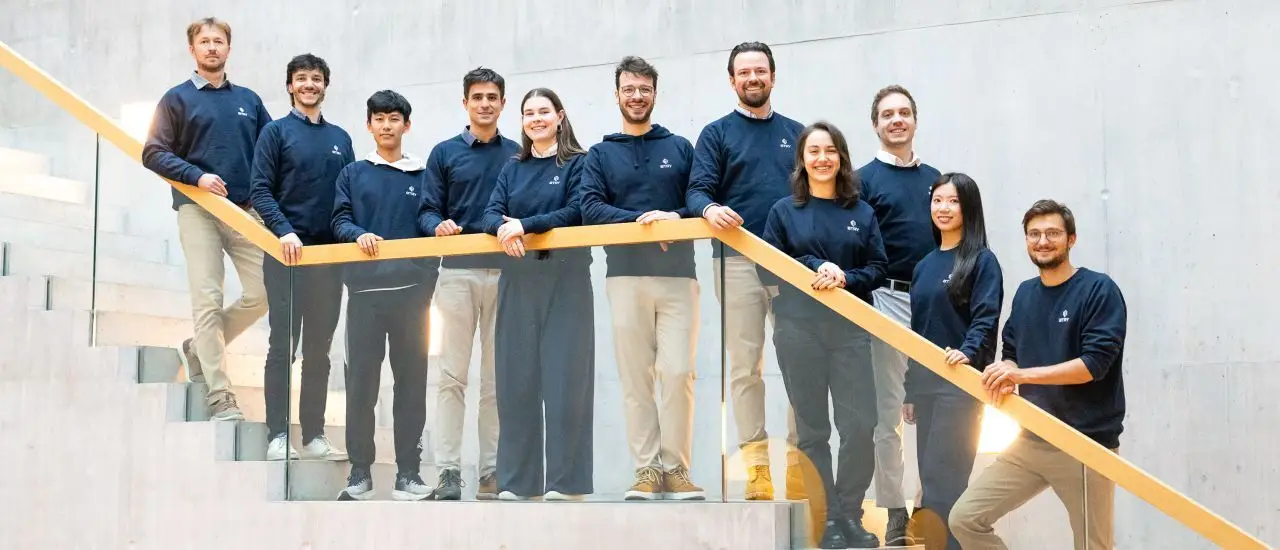
Today, Microsensys, led by managing directors Reinhard Jurisch, Peter Peitsch, and Sylvo Jäger, is once again on the verge of an important product launch. The first customers are already testing the new generation of mic3 transponders.
With dimensions of just 1.8 x 1.8 x 0.5 mm³, they are among the smallest on the market. They will be available in an identical format as both HF and UHF variants, each with different functionalities.
Over the past years, Microsensys has made a name for itself as a driving force of innovation in the RFID sector. This interview explores the origins of RFID transponder miniaturization, a development decisively driven by Reinhard Jurisch.
How did it all begin? What role did the divided and later reunified Germany play? And why was George Perlegos, founder of ATMEL, such an important figure in making this groundbreaking idea a reality?
How It All Began Over 40 Years Ago
By the way, the continuation of this success story will be published soon, focusing on HF and UHF technology. Which frequency band offers the greatest advantages for miniaturization? In the second part of the interview series, Reinhard Jurisch will shed light on the context surrounding this crucial frequency question. Discover the current mini tag series from Microsensys on the official Microsensys product page.
Interview
Why was the miniaturization of transponders the actual reason for founding Microsensys?
Reinhard Jurisch: The vision of miniaturizing electronic components has been a central idea that has fascinated me throughout my life. In the beginning, this goal was closely connected to my work. I was employed at VEB Kombinat Mikroelektronik Erfurt in the semiconductor industry, where I focused on circuit design and technology development for microprocessors and non-volatile memory.
In the semiconductor industry, everything revolved around scaling and miniaturization, with Moore’s Law serving as the main driving force in this field.
Smaller dimensions meant higher integration density, greater functionality, and lower power consumption. This concept has shaped my professional journey from the very start. However, greater functionality usually also required more complex communication interfaces, pins, and packaging.
The idea of wirelessly transferring energy and data had the potential to simplify many of these challenges. Ultimately, this was the reason behind the founding of Microsensys.
What was the original idea behind miniaturization?
Reinhard Jurisch: I always knew that if data carrier and communication chips were to become truly small, the antenna had to be integrated directly onto the silicon. The challenge was to bring all electronic components together on a single silicon chip.
For me, miniaturization remains a key driver of innovation to this day. Whenever I can miniaturize something, I know I am moving toward the future. Of course, there are other factors that drive innovation as well. Topics like wireless technology and low power have fascinated me from the very beginning. Miniaturization typically saves resources automatically, both during manufacturing and later in operation, thanks to lower energy consumption.
Would your vision of miniaturization and battery-free transponders have been possible without non-volatile memory?
Reinhard Jurisch: Non-volatile memory was a crucial element back then for storing data and making computer programs more flexible, and it remains just as important today. At that time, development was still in its early stages. Initially, there were memories that could be erased using UV light. Later, electrically erasable memories (EEPROMs) were introduced, which marked a decisive step forward.
Especially for transponders without a battery or their own energy source, it was essential to be able to store data reliably. Non-volatile memory was therefore the foundation. My vision was built on this type of memory combined with the idea of integrating everything on a single silicon chip.
How did the development progress from discrete components to integrated data carriers in the 1980s?
Reinhard Jurisch: Back then, everything was still built from discrete components: the antenna coil, rectifier, voltage generation, memory, transmitter, and receiver — each component separate.
All of these were housed in a small capsule with a diameter of about one centimeter and a height of five millimeters, which was already considered quite small for that time.
During this period, the first ideas emerged for car keys, animal identification, and data carriers for tools.
My employer at the time had just started developing EEPROM memory and the first 16-bit microprocessors. So I asked myself, "Why not also wireless data carriers?"
In the 1980s, no one was talking about RFID or radio frequency identification yet. These devices were simply called transponders or data carriers, and they operated at a relatively low carrier frequency of about 125 kHz.
By the late 1980s, my idea was clear: all of this must fit on a single piece of silicon. The remaining challenge was the antenna, which at the time was always a coil for the LF range. The key question became: How can I integrate this coil into the chip? That was the starting point.
Wasn’t it almost crazy to try to integrate a coil on silicon in the late 1980s?
Reinhard Jurisch: At that time, wafers were just two inches, or about five centimeters, in size. We then moved toward three-inch and four-inch wafers. The idea was to manufacture the entire transponder process, including the antenna, directly on a silicon wafer.
What impact did the fall of the Berlin Wall in 1989 and the reunification of Germany have?
Reinhard Jurisch: In 1989, I asked myself: "What should I fundamentally do with this idea that was already fairly well developed?" Should I stay in the semiconductor industry, or should I implement my vision independently?
With the political changes, I was able to travel freely for the first time. One of my first visits was to Prof. Herbert Reichl at the Technical University of Berlin. At the time, he was researching "technologies of microperiphery", meaning the assembly and interconnection technologies of microelectronics.
He encouraged me to file a patent for my idea, which I promptly did. The patent later became known under the numbers EP 0 507 903 and US 5,308,967.
We called the process mic3® (monolithically integrated contactless coil-on-chip technology). This patent became the foundation for the company. Together with Peter Peitsch and Dr. Olaf Brodersen, I founded Microsensys in 1991 in Erfurt.
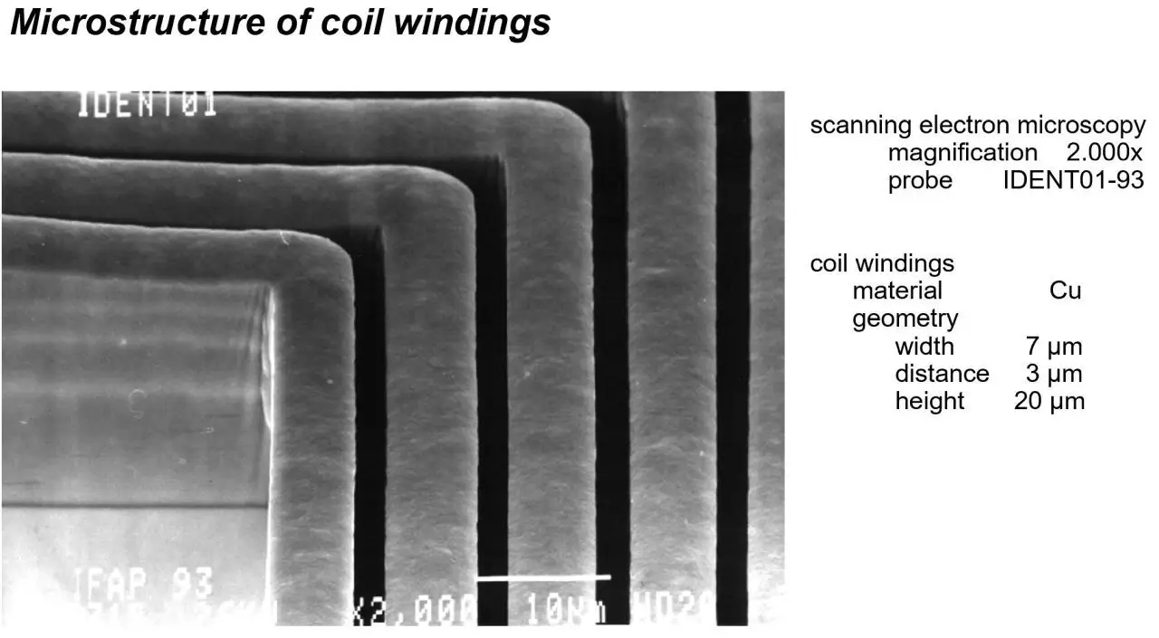
6 µm Wide and 20 µm High – Was this the patent idea for integrated coils in the semiconductor process?
Reinhard Jurisch: We considered how to implement an antenna coil for an integrated transponder and carried out initial simulations. It quickly became clear that a coil made from the standard metal tracks of conventional semiconductor processes would not achieve the required antenna quality for transponders.
To achieve a high number of turns and high quality, the tracks had to be not only very narrow but also unusually tall. Specifically, we needed conductor tracks with a width of 6 µm and a height of 20 µm.
Would your development after 1989 have progressed the same way in the GDR as it did later in reunified Germany?
Reinhard Jurisch: No, it would not have progressed the same way. In the beginning, many prerequisites were necessary, especially suitable silicon technology, meaning semiconductors. That was my area of expertise.
What we needed was a mixed-signal design that combined analog, digital, and high-frequency elements, as well as non-volatile memory cells. At that time, such capabilities were only available to a very limited extent. Maybe we could have achieved this years later, but whether I would have ever received the green light from our general director for such a project, I honestly don’t know. Probably not.
With reunification, everything changed. Suddenly, all doors were open to us, and we were free. I seized the opportunity and traveled extensively to find a wafer foundry capable of producing our silicon design. During this search, I eventually met George Perlegos, the founder of ATMEL and a pioneer of non-volatile memory.
How did the collaboration with George Perlegos go?
Reinhard Jurisch: George was in the process of upgrading his 2-kbit EEPROM to a new technology level that allowed high clock frequencies and enabled a mixed-signal design, including rectifiers for the high-frequency range. I was able to get him excited about the idea of a fully monolithic integrated transponder.
He provided us with the design rules for his process, which allowed us to do what we had already done ten years earlier: design circuits in silicon. The company MATRICS Ltd. in the UK completed the layout and created the GDS2 tape, which was then sent to ATMEL in Colorado, where the actual production of the wafers took place.
The chip size is no longer impressive by today’s standards: 4 x 4 mm². However, a photo of the chip along with the original layout still hangs on the wall in my office today.
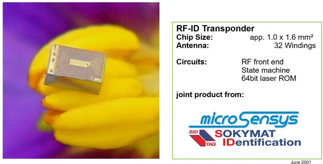
By the end of 2010, additional chips were developed and produced at ATMEL. One very popular chip was the AT88RF001, which was suitable for mic3® and featured an I²C interface for creating passive wireless sensors.
Well-known products based on this technology include the Microsensys' TELID®200 sensor transponder series.
How did production start in the early 1990s?
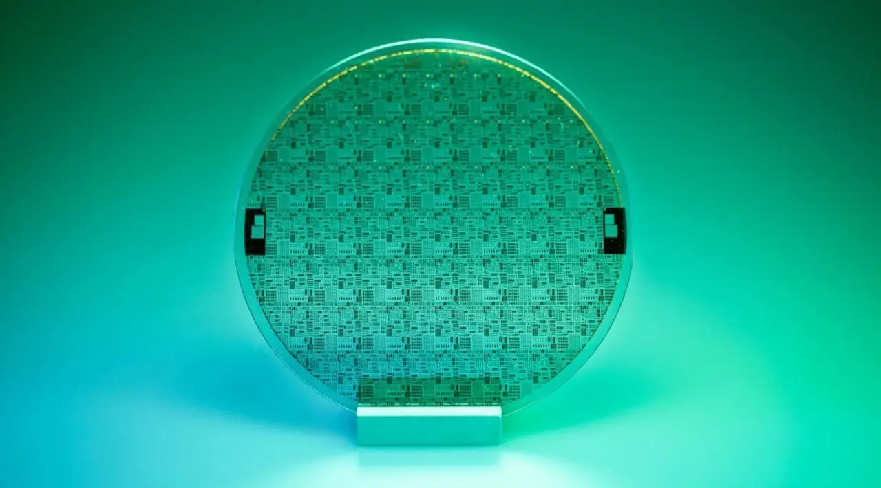
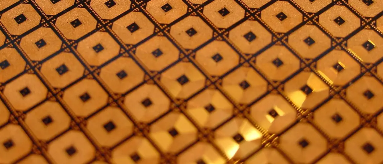
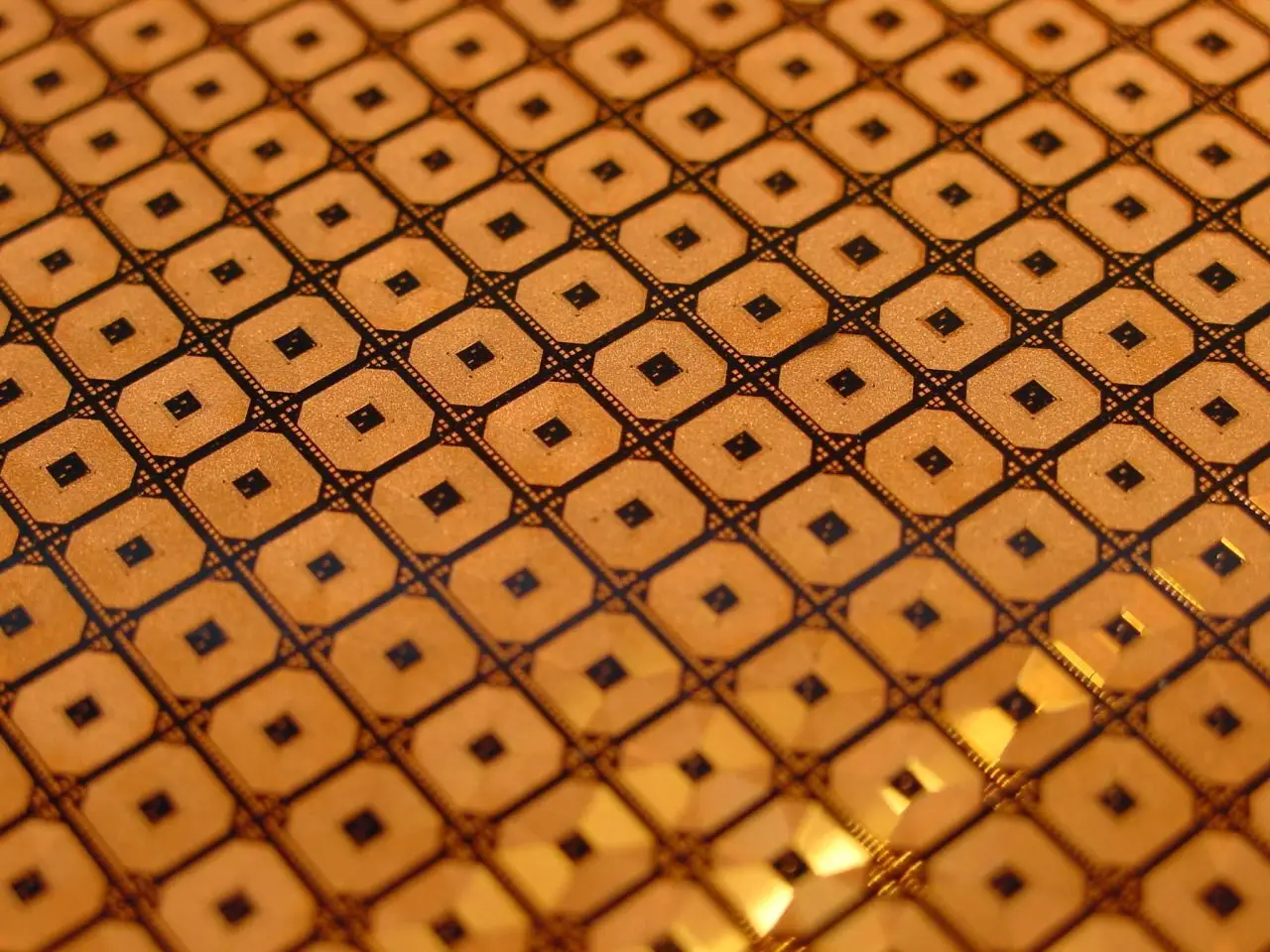
Reinhard Jurisch: ATMEL sent us the first prototype wafer — a 6-inch wafer with our layout and the necessary provisions to allow us to further process the wafer in our lab. Initially, there were around 1,200 chips on it, which, after the Mic3 preparation, were contactless and fully functional.
It should be noted that with the advancement of chip technology, we were eventually able to fit 8,000 transponder chips on a single wafer.
To protect the coil, the wafers were coated with a passivation layer and then sawn apart to separate the chips, just like it is still done today, 30 years later.
In 1993, we brought the first fully monolithic integrated transponder to the market. That was a world premiere. Since then, Microsensys has been offering the patented Mic3 technology, featuring one of the world’s smallest RFID transponders with a volume of just 1.5 mm³.
It should also be mentioned that, alongside our collaboration with ATMEL, there were other partnerships and different chip types. Notable among these were projects focused on the smallest chip in a 64-bit read-only version, with a transponder volume of just 0.8 mm³, based on silicon from EM Microelectronic Marin and realized with the support of SOKYMAT Identification SA.
One of the most advanced chips developed using the mic3 technology at the time was based on a wireless crypto chip from INSIDE Contactless, France. The chip featured a 32-kbit EEPROM, a crypto controller, and a fully compatible ISO-15693/14443 RFID frontend. It was intended for highly demanding applications. This was also a clear example of miniaturization, as the complete transponder, including the antenna, had a thickness of only 180 µm and a total volume of just 0.6 mm³.
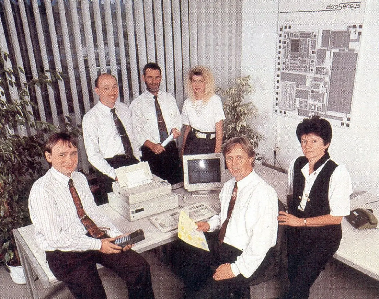
How was production at Microsensys set up? The company was just starting out, and German reunification had only been two years earlier.
Reinhard Jurisch: To implement the Mic3 technology, we needed wafers and compatible processing steps. Since all the founders of Microsensys came from the semiconductor industry, we knew exactly what needed to be done. It required a significant investment. Fortunately, we were able to secure funding through a support program called “Technologieorientierte Unternehmensgründung” (TOU).
We invested the money primarily in equipment and machinery, rather than in personnel costs. The idea was that once efficient production and sales began, we would be able to self-finance the company. Honestly, it took us longer to reach that point than we initially expected.
We procured semiconductor industry equipment: a mask aligner, plasma system, spinner, rinser-dryer, and built a small cleanroom, as well as a special electroplating unit — everything needed for wafer post-processing. The only difference was that we had to add just one additional functional layer, the coil.
We worked with exposure, coating, structuring, and etching. And then, amazingly, the first chip worked immediately. It received signals, generated its own energy, transmitted, modulated, and functioned exactly as intended right from the start — it was incredible!
What solution did you implement with the first transponders?
Reinhard Jurisch: Our first application was tool identification. At that time, there were companies such as BALLUFF, Euchner, BILZ WERKZEUGFABRIK, and others that we aimed to supply with our technology.
In parallel, there were already companies very interested in integrating the new, small chips into their own data carriers.
What were your competitors doing in the early 1990s? Was there a head-to-head race?
Reinhard Jurisch: In the early 1990s, not all competitors were immediately focused on full integration. Many companies initially concentrated on developing the basic silicon for transponders. Everyone was experimenting with silicon, but always with two bonding pads and an external antenna.
In the case of smart cards, the foil layer carried the antenna coil.
Of course, many manufacturers developed their own silicon for transponder applications until, eventually, semiconductor companies took the lead in design. At that time, the main focus areas were contactless smart cards and label production for applications requiring a longer communication range.
The design always relied on three parts plus additional assembly processes:
Chip
Carrier foil
Antenna
This effort was greatly reduced with the Mic3 technology, but as a trade-off, the communication range was also reduced. Back then, this was not very popular.
At the end of the 1990s, Hitachi also entered the market with a coil-on-chip technology. Initially, this seemed like a problem for us. However, it turned out to be beneficial because a corporation of that size could generate much broader marketing reach, which helped the topic of miniaturization gain momentum again.
In addition, our patent prevented others from creating chip antennas with the same transmission characteristics as Mic3.